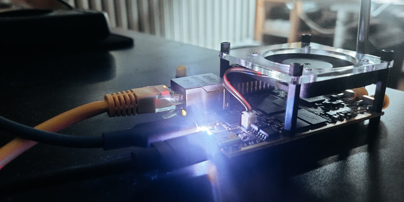
Wiring up the RX digital interface
With the hang from the last post resolved, I finally had a stable enough platform to start on the part of this project I actually care most about: getting real samples out of the AD9361. First step was wiring ad9361_if_rx.sv — the RX-only LVDS digital interface — into the top level, which meant I needed the chip’s digital and ADC sample-rate logic actually clocked before any of it would do anything useful.
That clock comes from the BBPLL, the AD9361’s internal PLL. On this board, it needed to lock at 960MHz starting from a 40MHz external reference. The datasheet here was my friend, up to some point. It was huge documentation, but honestly missed some of the low level details I wish it had. So the only thing I can really do is proceed and implement to the best of my understanding a routine via SPI to bring-up the AD9361.
That discipline caught two real bugs before either one cost me hardware debugging time.
Two bugs caught before they became hardware mysteries
The first was a power-on-reset default bit, REF_DIVIDE_CONFIG_1_DFLT, that a full-byte UART write was silently clearing on its way into the register. The effect was subtle and nasty: BBPLL_LOCK would never assert, no matter how many times I retried VCO calibration, because the bit governing part of the reference path had quietly been zeroed by a write that was never supposed to touch it. Full-byte writes to registers with meaningful default bits are exactly the kind of thing that looks harmless until it isn’t.
The second was a missed XO_BYPASS requirement. This board drives the AD9361 from an external reference clock rather than its onboard crystal, and the chip’s “default” clock-enable configuration assumes the opposite — the onboard crystal path. Tracing the actual driver source made that assumption visible in a way the datasheet’s field descriptions alone didn’t.
With both fixed, I confirmed the RX clock-divider chain on real hardware with the most reliable test ever conceived: driving an LED off a dsp_clk-domain counter and measuring the blink period with a stopwatch. Two configured rates, 15MHz and 30MHz, both matched the derived divider math to within measurement noise. Not an elegant instrument, but a real one — an LED that blinks at the rate you calculated is a surprisingly hard thing to fake.
The wall
Then I hit it. REG_STATE reached ALERT (0x05) — correct, exactly where I expected the AD9361’s state machine to be at this point in bring-up — but going any further, to the real RX state, needed a completely separate PLL that I hadn’t touched at all: the RX local oscillator synthesizer.
I left enter_mission_mode() in my FW in the codebase as a deliberately empty stub, with the known-so-far sequence sitting in a comment rather than in code I wasn’t ready to trust yet. In the meantime, test mode worked fine — a chip feature called ENABLE_RX_DATA_PORT_FOR_CAL appeared to force the RX data port active without needing the full state transition at all. Good enough to keep testing the digital interface while the real synth bring-up waited.
I didn’t know it yet, but that “test mode works, mission mode is blocked on the RX synth” line was the setup for the longest single day of the whole project so far. ENABLE_RX_DATA_PORT_FOR_CAL looking like it worked was about to turn out to be one of the more interesting red herrings I’ve hit on this board. That’s next.