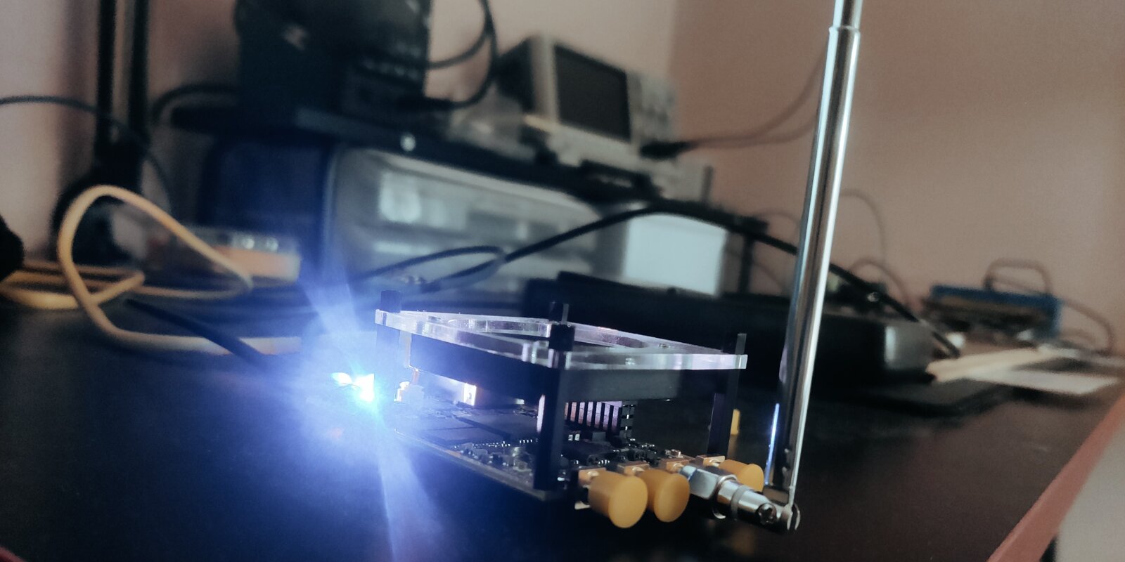
A new project: building a Pluto clone from scratch
After the RISC-V detour, I’m back on the RF side of things, which is really where this whole hobby started for me. The new project is fm_receiver: a Zynq-7020 SDR receiver built around a HamGeek board carrying an AD9361 — the same RF transceiver chip at the heart of Analog Devices’ own ADALM-Pluto. Custom AXI peripherals, bare-metal Cortex-A9 firmware with no FSBL, no BSP, no OS, and an AD9361 bring-up sequence I’m deriving register-by-register against ADI’s own reference driver rather than copying an example project. Pure non-project batch-mode Vivado throughout — I’ve never once created a .xpr file for this. I’ll be documenting it here the same way I documented the CPU build: as it actually happens, wrong turns included.
The risk budget: why the PS7 didn’t get hand-derived
Everything else in this project — RTL, AXI peripherals, constraints, software — is getting written from scratch. The one deliberate exception is the PS7, the Zynq processing system block that configures clocks, the DDR controller, and MIO pin muxing. I inherited that block from a HamGeek vendor reference project instead of deriving it myself from the schematic.
That’s a real double standard, and I want to be honest about why I made it. DDR3L timing and MIO/clock parameters are genuinely risky to get wrong by hand — get them slightly off and you don’t get a clean failure, you get a board that’s flaky in ways that are brutal to diagnose, because you can no longer trust the platform underneath whatever bug you’re chasing. Everything else in this project is worth learning by re-deriving it myself. The PS7 configuration is not one of those things; it’s exactly the kind of parameter set a vendor has already validated in silicon (like delays from DDR to PS, among other things), and re-deriving it from scratch would have bought me risk without buying me understanding.
First real task on the inherited design was mechanical: upgrading it from Vivado 2021 to 2025, which meant regenerating the PS7 IP cell to the newer revision. Then the obvious blinky LED… this was not that immediate however. Blinking the LED in pure PL is a trivial bitstream upload, what I needed was to know that I have control of this LED state via
PC->UART->PS store instruction->AXI->PL
Without this, I wouldn’t be happy.
The AXI bug that simulation could never have caught
The first real hardware milestone broke immediately. I’d wired a hand-written axi_interconnect — a simple 1-master/N-slave AXI address decoder yet the basis for all the configuration of this project — between the PS7’s M_AXI_GP0 port and the peripheral cluster. Remember, the catch is pure RTL, no Vivado flow, so I’m writing my own AXI bus as a learning experience. The moment I loaded the bitstream, the entire UART register console I made for reading any AXI request went silent. Two independent bugs, stacked on top of each other.
The first was missing AXI ID routing. My interconnect routed ADDR/LEN/SIZE/BURST and the data/response channels correctly, but never touched AWID/ARID/WID/BID/RID — I’d hardcoded BID/RID to zero and called it done. A real AXI3 master enforces that the BID/RID it gets back matches the AWID/ARID it sent out on the request. PS7 does exactly that, and it stalled forever waiting for a response tag that would never arrive, because I’d never generated one. This is invisible in simulation unless your testbench specifically models a real master’s ID-matching behavior — mine didn’t, because I’d never had a reason to think about it. It only ever showed up against actual silicon.
The second bug was a peripheral sitting in dead address space. I’d placed axi_spi at 0x8000_0000, which — per the Zynq-7000 TRM’s fixed system-level address map — belongs to M_AXI_GP1’s window. My design only ever wires up M_AXI_GP0, which covers 0x4000_0000–0x7FFF_FFFF. The address wasn’t wrong in any way RTL or timing analysis could ever catch; it was categorically unreachable from the PL side, a fact that lives entirely on the PS side of the boundary, before an access ever reaches PL logic at all.
The generalized lesson stuck with me for the rest of the bring-up: anything that depends on real AXI master behavior, or on the PS/PL address split, is invisible until you’re on actual hardware, no matter how clean your simulation looks.
A floating pin holding the whole chip in reset
Separately, and just as instructive: the AD9361 was returning 0xFF on every single SPI register read, no matter which address I queried. The root cause was almost embarrassing once I found it — gpio_resetb, the AD9361’s active-low RESETB pin, had never actually been wired to a top-level port in fm_receiver.sv. Floating, it held the chip in reset with a dead SPI interface the entire time I’d been debugging the interconnect. One added port and one assign line later, REG_PRODUCT_ID read back correctly — 0x0A, matching the expected product ID and silicon revision — and a write/readback round-trip on a second register confirmed both SPI directions worked.
It’s a nice contrast to the AXI story: not every hardware bug is a subtle protocol-compliance issue buried in the standard. Sometimes it’s “you forgot to plug in the reset wire.”
With the LED blinking at my command, SPI alive and the register console I built via UART talking to real silicon using an AXI bus, the project had its actual starting line. What came next was a bug that took a lot longer to run down — a hang that would only show up after the board had been running for a while, and that took ruling out most of the ARM core’s own errata before the real cause turned up somewhere nobody was looking. That’s next.