Introduction
Perhaps it’s only me, but I believe anyone who is serious at digital design should at least try to implement a simple processor. This is the first of a series aimed to end with a usable processor for my projects, in an attempt to learn some of the concepts of computer architecture, while at the same time honing my hardware design skill. This post is a technical overview of the design choices behind it: where I made reasonable calls, where I got it wrong, and what I learned along the way.
Why single-cycle, why RISC-V
Out of every digital machine you could build, a CPU is arguably the one with the most day-to-day impact on people’s lives — not necessarily the most complex circuit out there, but the one that’s everywhere. I’d read Hennessy & Patterson years earlier, but only recently got my hands on hardware to actually build one. Rather than follow someone else’s RTL, I extracted the logic directly from the RISC-V unprivileged ISA specification, trying to guess at the right microarchitectural blocks as I went. Decoding the spec into hardware — not writing the Verilog itself — turned out to be the real challenge. So single cycle is the most spontaneous piece of hardware that can test my understanding and the correctness of my implementation. As to why RISCV, simply because it’s open and simple, the 32bit integer specification is no more than 20, quite detailed, pages you can find at the unprivileged specification
The project: SystemVerilog, targeting my Arty A7 board. I haven’t run it on real hardware yet — everything so far has been verified in simulation and disregarding for now about timing optimizations.
Verification approach
For the smaller building blocks (register file, ALU, memory), I wrote basic self-checking testbenches. For the datapath as a whole, I built one big self-checking testbench that ran actual programs — compiled with a real RISC-V toolchain, not hand-written instruction sequences — and checked that memory ended up in the state the program expected. Working from a real compiled binary instead of hand-picked instructions caught a class of bugs that manually-crafted test vectors would have missed entirely.
| |
While not extensive as the real tests, it will stress many tricky instructions like the conditional branches and jal/jalr requirements.
Block diagram
Before getting into individual blocks, here’s how they connect in the single-cycle datapath:
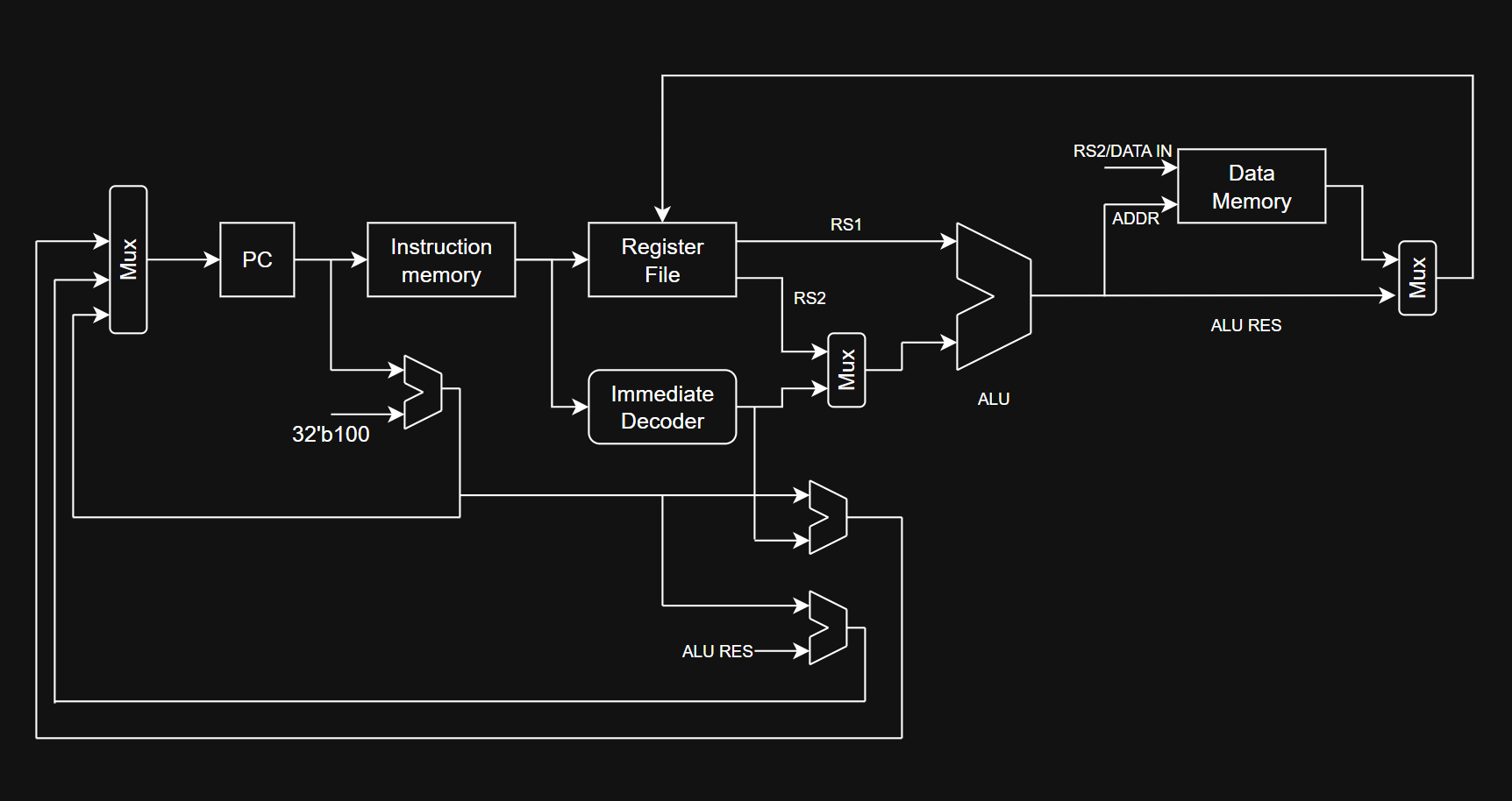
Block diagram of a single cycle RISCV without control unit
At a glance: the PC drives instruction fetch, the control unit decodes the instruction into every downstream select signal, the register file and immediate decoder feed the ALU, and the ALU’s result branches out to either data memory (loads/stores) or back into the register write-back mux — all within a single clock cycle, which is exactly what makes this a single-cycle design: no pipeline registers, no stalls, just one long combinational path from fetch to write-back on every clock edge.
Design choices
Program Counter
The PC is about as simple as sequential logic gets, but it’s a good entry point into how control flow decisions ripple through the datapath:
| |
pc_src is a 2-bit control signal that selects between four sources for the next PC value: sequential execution, JAL’s PC-relative jump, JALR’s register-relative jump (masking bit 0 per spec), and conditional branches gated by the ALU’s branch output.
Note the two dedicated adders, pc_plus4 and pc_plus_imm, sitting right next to the ALU. That wasn’t the first version of this design — more on that below.
Register File
| |
Two read ports (rs1, rs2) decoded combinationally straight off the instruction fields, one write port gated by wen. The one detail worth calling out for anyone implementing this for the first time: register x0 has to read as zero and stay zero on writes — the spec requires it, and it’s an easy thing to forget to enforce on the write path specifically, since the read path naturally returns whatever is stored at index 0.
Data Memory
| |
Memory is modeled as a byte array, with d_width selecting byte/halfword/word access and mem_signext controlling sign- vs zero-extension on loads — directly mirroring RISC-V’s LB/LBU, LH/LHU, and LW distinctions. Writes follow the same width logic on the synchronous side. This was my first pass at a memory block, so it’s more of a working baseline than a polished design — but it got the datapath running correctly against compiled test programs.
The AUIPC lesson: not everything belongs in the ALU
The one moment that really stuck with me: I got stuck trying to make AUIPC work through the ALU, treating it like just another instruction that needed op1 + op2 in the same functional unit as every other ALU operation. It didn’t click for a while that PC-relative addition doesn’t have to go through the ALU at all — it’s arguably not even an “ALU operation” conceptually, it’s PC arithmetic.
The fix ended up being the two dedicated adders you can see in the PC section above: pc_plus4 for sequential fetch and pc_plus_imm, reused for both AUIPC’s PC + imm and JAL’s target calculation. Once I stopped trying to force every addition through one shared unit, the design actually got simpler, not more complex — a dedicated adder is cheap, and it decouples PC-relative arithmetic from whatever the ALU is doing that cycle.
It’s a small thing, but it’s the kind of assumption (“reuse the general-purpose block for everything”) that’s worth questioning early — especially coming from an analog background where dedicated, purpose-built circuits are often the default instinct anyway.
Conclusion
This single-cycle design became the baseline for the pipelined RISCV32I CPU I’m currently building — same ISA, same lessons carried forward, very different set of problems. That comparison is next up.