
Introduction
It took me a while to come up with worthy content, but here I am. I have been working on getting my FPGA board to sample analog audio with the internal ADC for a project proposed by a colleague as a way to learn the intricacies of digital design. Let me tell you straight: the documentation for the ADC on this Artix 7 device does a great job of being confusing. I’m not ashamed to say that this is the part that took me the longest to figure out, also considering my paranoia about damaging the components with non-compliant voltages.
So, before starting on the actual implementation of this effect/filter chain in an FPGA, let’s agree on some architecture. Given my limited experience with this kind of project, there’s a lot I found could be done better. But for starters, this will work.
Effect Chain Architecture
Let’s set some constraints for the design of this architecture1:
- I want a 48KHz sample rate for the audio, to use my already-designed I2S interface
- I want the maximum sample rate possible from the XADC (per the documentation, 12-bit at 1MSPS)
- I want to avoid clock cross-domains, hence the same clock will have to drive the ADC and the I2S interface
The third constraint is tricky, because the XADC takes 26 clock cycles2 to sample the input, so if I wanted 1MSPS, I would need a 26MHz clock. However, I also need a 48KHz clock/strobe for the I2S and the audio processing chain in general. Considering the PLL in the Artix 7 device can’t go below 10MHz, I will have to strobe the audio chain off the same clock as the ADC while also making them synchronous (an integer number of samples from the XADC processed per 48KHz period). For this reason, I will choose the PLL frequency as 60MHz, set the divider on the XADC to 3 (hence it will have an internal clock of 20MHz), and set the divider of the audio chain to 26*48 = 1248. This gives the audio chain a sampling rate of 48076.92Hz. Close enough, no one will notice.
Still, there is the discrepancy between the sample rate of the XADC (about 770KSPS) and the 48KSPS we want for audio processing. But that’s easy to fix, and it comes with benefits: let’s just add an accumulator that sums 16 samples. So basically, we accumulate 16 samples of the XADC with two benefits:
- It reduces the noise of the analog front-end and XADC by applying low-pass filtering
- It increases the resolution of the data from 12-bit (XADC samples are 12-bit) to 16, which I like more.
So, we could draw up a block diagram for the system as follows:
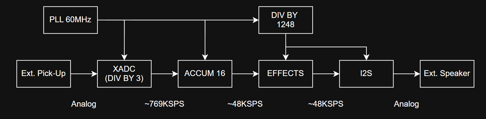
Block diagram of the effect chain architecture
In this post, I’ll just briefly outline the XADC configuration — in case you find this while trying to sample with it, as I did — and the accumulator code. In the next articles I will be covering the following pieces:
- Analog front-end design
- Finite Impulse Response (FIR) filter digital design
- Control unit for a pseudo register map implementation and UART communication
- Routing system for the effect chain
- Brief discussion on the effects that will be created
At the time of writing, I have everything but the last two points — hopefully by the day I start writing about them, I’ll have completed the project.
Quick XADC snippet
As mentioned before, the documentation is fairly complicated to navigate, and it took me a while to figure this out, so I’m just giving you a recipe to start with the XADC for your own projects. I have put the most important comments in the code to set it up properly. For the internals, use the wizard for single-channel, continuous sampling from the analog pins as set in the design constraints file.
Set the other settings as you like — they aren’t important at all. As I don’t need the extra complication of an AXI bus, I will stick with DRP.
| |
Accumulator implementation
This is nothing fancy: we use the main clock and a carry adder to accumulate samples until it counts 16 steps, then provide the result to the output along with a sample_ready signal. We can do this really quickly without timing issues in the available sampling time of the XADC (1.3us), so a simple strategy is better. The XADC even provides a sampling_done signal we can use to avoid wasting transitions on this little block.
Here is the snippet:
| |
Now, if you’re paying attention, you will see the input of the accumulator is 16-bit, not 12-bit. Well, it just happens that the XADC provides 16 bits, where the 4 LSBs are declared for “averaging” — which is what we’re doing right here. Still, I will be keeping the 16-bit output. For my purposes, this will give me enough resolution for all the computing I have to do on the guitar audio.
Conclusion
Here we have the beginning of a hobby project I’ve been dreaming about since childhood: my own guitar effects. We set the strategy and the next steps to make it a reality.
Stay tuned.
As the good master Aloys said in Fux’s book: the mastery of the rules is the way to artistic freedom, it’s within the constraints that real creativity is born. ↩︎
I would infer it’s a SAR ADC, so 12x2 clocks for comparator/feedback, plus 2 to propagate the sample to output. But this is conjecture from my side ↩︎