Introduction
Last time, we built a circuit together using Verilog to communicate with an I2S device. But we never delved into how to make a waveform for it.
Now, don’t get me wrong: if you did the blinky LED example when starting your first projects, this should be easy for you:
- A square pattern is just zeros and ones
- A saw pattern is a counter from zero to max
- A triangle wave is a counter that goes back after hitting max or min values
- A sine wave is just some CORDIC…
Now, we will not be using CORDIC and will not be doing simple counters. I want to show you a couple of tricks to generate a clean sine waveform that you can later compose to create fancier sounds.
Single LUT1
Instead of CORDIC, we will encode the values of the sine function within a lookup table (LUT) and then use and transform those values as needed. This will allow us to create a shape that resembles the trigonometric function, just without frequency content. Instead, for the frequency we will use a counter and call it a phase accumulator because it sounds better. This counter will keep track of the phase per time step (clock or strobe), hence the frequency will directly be a ratio between the phase advancement and this time step.
Sine ROM
Let’s take a look at the ROM:
| |
Here, I encoded the values of the sine function from zero to pi/2. This is because, to save memory and resources, we’d rather leverage the sine’s symmetries and do a little calculation depending on the phase.
The resolution of this function is 8-bit and there are 64 values. This means that, using the symmetries, we add a sign, making a 9-bit value for a total of 256 samples per period. If we use the same sampling rate as in the earlier I2S post — 48KHz — a full period comes out to 48KHz/256, or 187.5Hz. This basically defines the frequency resolution, and as such, I don’t like this number. So I will artificially boost the number of samples in the LUT by using linear interpolation. At the same time, this interpolation boosts the resolution of the signal by a few extra bits, at some penalty to the Signal to Noise plus Distortion Ratio (SNDR) compared to using a bigger, more accurate LUT — but with huge savings in power, area, and complexity.
Synthesizer
We use this sine ROM with a circuit that fetches the values by encoding the phase into a memory address, and transforms them into a complete waveform. So let’s put together a framework to begin with:
| |
As inputs, we have a clock — which, for compatibility with the I2S circuit, will be 60MHz — a volume control, and the phase step per time step (a proxy for frequency). As output, we provide the current value of the numerical oscillator.
Let’s see how to turn this quarter-wave into a complete wave:
| |
Not sure how intuitive this is, but basically two things happen here:
- On even quadrants, the address into the ROM flips to the other side to maintain continuity after pi/2 and 3pi/2.
- On the third and fourth quadrants, the sine changes sign, so we add this sign and transform into a two’s-complement signed value.
Then, via synchronous logic, we update the strobe (to convert from 60MHz to 48KHz) and the phase accumulator, and keep track of the last value of the ROM. Consider that we will move only forward in phase here.
| |
You can see that data_last changes only when the data calculated from the ROM values changes. This value will be used for linear interpolation.
Linear interpolation
Let’s be blunt here, because either you know what it is or you don’t: between two points on the sine table, we draw a line and divide it into a power-of-two number of slices. This is not necessarily a good approximation, but the quantization error is much smaller than doing nothing at all.
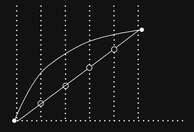
The white dots are the values in the LUT, the curve is the theoretical values of the function in continuous time, the black dots are inferred from a line between the white dots.
The values at the midpoints between two values of the LUT follow a simple linear relationship. Basically, divide $\Delta Y$ by $\Delta \phi = X_{n+1} - X_{n}$ to obtain the slope, then multiply by the current slice in the phase and add the last value:
$$ Y = Y_n + \frac{Y_{n+1} - Y_{n}}{X_{n+1} - X_{n}}m $$
here, $m$ is the current slice between two points in the LUT. We will choose a power of two for the maximum value of $m$ for simplicity, but it can be any value. The trick here is that the maximum value of $m$ is equivalent to the number of slices between $X_{n+1}$ and $X_n$, and if this value is a power of two, the division becomes a right shift. Actually, we don’t even have to do this shift, as the data is 9-bit (8 + 1 for sign) and we extended it by an additional 15-bit up to 24-bit. Hence, we can just leave it as is and call it a day. Then, what we do instead is leverage the 18-bit phase accumulator and split it as follows:
- bit
[17:16]tracks the sine quadrant - bit
[15:10]tracks the address in the sine ROM - bits
[9:0]are used for interpolation
So we can take the 18-bit data with its extra headroom, shift back 10 bits, subtract, then multiply by the interpolation partition that tracks the current slice between two ROM points. The data is already shifted, so that’s fewer circuits for us.
With 10 bits of interpolation, we are converting the 8-bit ROM data into 18-bit, adding one bit for the sign, and then we can multiply this value by the volume setting, getting a total of 24-bit data for the I2S circuit.
Neat, isn’t it?
One more note about the interpolation: by using multiplication with this recipe, we are leveraging the DSP slices in the Artix 7 FPGA. There are something like 120 or so of those slices, so they’re kind of precious, and it’s better to save them for critical calculations. In this example we just used two of them for a synthesizer.
Conclusion
This is just a toy example of how to build a LUT-based synthesizer. More improvements can be made, and perhaps I will. You can send this 24-bit data and chain it with the I2S circuit we did last time, put on headphones, and listen to the result.
As usual, if you want to get the sources of these blocks, as I write this blog I’ll place them at my GitHub repo
Disclaimer: don’t abbreviate the word “Single” please. ↩︎